Semiconductor Economics: China Bypasses EUV Ban With Costly Trade-offs
Chinese fabs are leveraging multi-exposure DUV techniques to close the gap with Western leaders, but experts warn that yield rates and production costs are climbing significantly.
By Imani Brooks ·
Morgan Stanley projects that Chinese chip self-sufficiency will jump from 42% in 2025 to 70% by 2030, a shift that relies heavily on advanced packaging and existing deep ultraviolet technology. This strategic pivot allows domestic manufacturers to maintain growth despite the continued exclusion of extreme ultraviolet machines from the Chinese market. While the progress is notable, industry analysts emphasize that this independence comes with a steep price tag in terms of efficiency and cost.
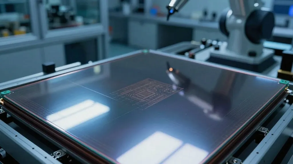
The primary obstacle remains the lack of access to EUV lithography systems. These tools, manufactured exclusively by ASML, utilize 13.5nm wavelength light to etch the finest details on modern processors. With the EUV gap estimated at five years or more compared to Western rivals, Chinese foundries are relying on older DUV equipment. By exposing critical layers multiple times, these machines can produce capable silicon, though the process is far less efficient than a single EUV pass.
Recent advancements demonstrate that this workaround is viable. A 2023 teardown of the Huawei Mate 60 Pro revealed that the Kirin 9000S chip was manufactured using a second-generation 7nm class process without EUV. More recent analysis suggests the newer Kirin 9030 has pushed DUV-based processes closer to 5nm density levels. While this trails the leading edge of TSMC and Samsung, it marks a significant step forward for domestic production.
The technique known as multiple patterning involves splitting a complex design into several simpler patterns and building the layer incrementally. Chris Mack, CTO of Fractilia, explains that industry wisdom previously suggested three exposures on a 193 immersion tool cost roughly the same as one EUV exposure. However, at four masks, EUV becomes the cheaper option. This shift in economics means that while DUV remains possible, the financial burden increases with every additional exposure step.
Quality control presents another major challenge. Each new pattern must align perfectly with previous etching steps, leading to accumulated overlay errors. Designers often add extra space around features to compensate, which enlarges the chip and reduces the number of dies per wafer. Since wafers cost tens of thousands of dollars, this loss of density is a significant financial hit. Mack notes that manufacturers ultimately sell die, not wafers, making this efficiency gap critical.
Memory production offers a clear view of this disparity. Morgan Stanley estimates that CXMT produces only about one-third as many bits per wafer as its Western competitors. Despite this, the bank believes CXMT can still increase its global DRAM bit supply share from 14% in 2026 to 16% in 2028 by adding new capacity. Similarly, researchers from Copenhagen Business School expect advanced packaging to allow firms to use DUV for the latest DRAM generations by the end of the decade.
While DUV has limits, it is not without precedent. Micron previously developed its 1-alpha DRAM without EUV, pushing 193nm technology further than other memory makers. However, Micron eventually transitioned to EUV for its 1-gamma DRAM to achieve over 30% greater bit density. Mack argues that without EUV, it would be difficult to make 3nm or 2nm nodes economically viable. For now, Chinese chipmakers will continue to accept larger dies and poorer yields while steadily expanding their production capacity.
Source: Tom's Hardware